Quality Control
Because Of Professionalism, Rest Assured.
FPGA Corp have our own perfect quality control system and professional team for supplier management, quality assurance, and customer service. All our products are completed traceability with strict ISO management system and quality testing requirements. Meanwhile, with 6S management standard, we develop our own warehouse management system WMS to make delivery fast and safer, no matter it is by air or by courier, all DHL, FedEx, UPS, SF express are available with flexible customs clearance option.
All our working principle is traceability of product information, traceability of workflow, traceability of position management, traceability of supply chain, traceability of quality control.
Supplier Management
Before new supplier making code in our supplying system, we must conduct market research with 6 indicators, after confirm qualified, then can approve to enter, which can select the best new suppliers and eliminate the inferior suppliers from the source.
After supplier registered in our system successfully, we will adopt a quarterly and annually evaluation from more aspects, supervise them to improve their service, and optimize supplier ability, and provide strategic support for procurement in following years.
If the supplier clearly violates the contract provisions or provides counterfeit and inferior goods, once discovered, we will not cooperate with forever and will use legal means to protect the legitimate rights and interests of ourselves and customers.


Quality Assurance
We provide one-stop testing service for components from pre-sale to after-sale, and help buyers and engineers to provide comprehensive and professional testing solutions in component selection and procurement to ensure the safe and efficient operation of the customer’s supply chain.
Our co-operated third party laboratory has rich qualifications and experience, and there are dozens of testing engineers (all from large platform companies, who have been working in the component quality testing industry for many years).
Common testing items can be issued on the spot results, provide efficient and professional and reliable testing services, escort your trade transactions while seizing the opportunity of trade procurement, and provide key customer service exclusive channels and solutions.
Test principle always insist: strict operation, strict inspection, serious verification.
Test Equipment
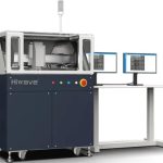
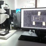
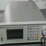
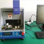
Our laboratory has a complete set of state-of-the-art component testing equipment, equipped with high-level and experienced testing personnel, and a strict quality control system to ensure that all goods provided are 100% brand new and authentic, and meet customer quality requirements. Our company can conduct various appearance and functional inspections according to customer requirements.
Test Standards
All tests conducted by FPGA Corp strictly follow the following testing standards. If the customer has any other requirements, please inform us in advance and our company will fully cooperate.
- IPC/JDEC Solid State Technology Association Standard
- GB/T2828.1-2012 National Sampling Standard
- IDEA-STD-1010-B Independent Distributor Alliance Electronic Component Quality Inspection Standards
- Datasheet
- MIL-STD-883 Experimental Methods and Procedures for Microelectronic Devices
- ISO9001 standard
- Customer requirements
- Gold Sample In Warehouse
Test Items
Our laboratory can mainly conduct the following 10 tests for electronic components:


- Test Scope: All kinds of components are original, whether refurbished, pin has no tin, oxidation and so on.
- Test Content: External visual inspection is the engineer according to the standard process requirements using high power microscope to sample packaging, label, tape, plastic texture, screen printing, pin technology, size, oxidation degree and so on a series of comparative inspection.
- Test Scope: It mainly checks the chip’s pin frame, wafer size, and gold wire binding map for internal structure delamination defects.
- Test Content: By using X-Ray to penetrate different density substances, its light intensity changes are different, and the contrast effect can form an image, which can show the internal structure of the object to be tested, so as to know whether there is a defect inside the chip without destroying the sample to be tested.
- Test Scope: All kinds of IC, active components pin/pad tin quality is up to standard.
- Test Content: External visual inspection is the engineer according to the standard process requirements using high power microscope to sample packaging, label, tape, plastic texture, screen printing, pin technology, size, oxidation degree and so on a series of comparative inspection.
- Test Scope: Used to check internal wafer information, wafer size, manufacturer logo, copyright year, and wafer code to determine the authenticity of the chip.
- Test Content: The cover is mainly used to corrode the package on the surface of the chip by using chemical reagents, which can expose the internal structure of the chip, so as to facilitate the direct observation of the authenticity of the manufacturer of the chip inside the wafer or provide intuitive detection and judgment for the analysis of the cause of failure.
- Test Scope: It is mainly used to write the program of the chip and write the data into the programmable integrated circuit.
- Test Content: Burning is completed by a burning device or a burning card. It refers to the use of a burning machine to burn data (also known as burning) to the burning disk, and write the program to the memory. Users can delete, check, program, check, encrypt and other common command sequences, and freely organize a single command.
- Test Scope: Detect delamination, cracks, air holes and adhesion conditions at different positions inside the chip module.
- Test Content: The non-destructive testing method is used to inspect the internal defects of materials by using the energy change of the reflection of the ultrasonic propagation waveform and the penetration time of the acoustic performance difference between materials and their defects. It can meet the different packaging types of Internal structure after scanning chip detection, mostly used to check the defects in the chip seal.
- Test Scope: Analyze whether the chip is a lead-free product and whether the content of harmful substances exceeds the limit value.
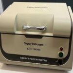
- Test Content: The X-ray fluorescence spectrometer is used to quickly and simultaneously determine multiple elements. Through the X-ray penetration of internal electrons in the atom, characteristic X-rays are generated by the outer electron supply. According to the intensity of element characteristic X-rays, the content information of each element can be obtained.
- Test Scope: By testing the electrical parameters of electronic products to determine whether they meet specifications and standards.
- Test Content: According to the device pins and related instructions specified by the manufacturer in the specification, the semiconductor tube characteristic diagram instrument is used to check whether the chip is damaged through open circuit and short circuit testing, and the normal working performance is determined by testing the electrical characteristics of the circuit.
- Test Scope: Generally observe the sample section structure, commonly used in PCB/PCBA and other parts.
- Test Content: Observe the internal structure and verify the suspected abnormal cracking and voids found in the sample by slicing method. Through physical grinding, to determine the layered structure of the components, whether there are structural defects. If the original sample is available, compare whether the internal layered structure is consistent.
- Test Scope: Detect the functional characteristics of the device, test the parameters, indicators and functions of the chip.
- Test Content: Under specific working conditions and normal working conditions of the device, various necessary logic or signal state tests are carried out to analyze the logic relationship of the signal and the change state of the output waveform, and the key functions of the semiconductor device are verified according to the original factory specifications and industry standards or norms.
Failure Analysis
If any minor issues or doubts are found through the above tests, our company FPGA Corp will follow the right principles for sufficient investigation, and finally propose corresponding error analysis and issue corresponding reports and solutions.
- Objective before subjective
- Outside before the inside
- Non-destructive testing followed by lossy testing
- First non-destructive analysis followed by destructive analysis
FPGA Corp Failure Analysis Methods
- Observe whether there are abnormal phenomena on the surface and bottom of the sample
- Observe whether the Pin foot of the sample has obvious abnormalities or falls off
- Check the distance, radius, Angle and size measurement of the sample
- Confirm the abnormal location and specific condition of IC, and make preliminary analysiscauses of failure
- Sample appearance and morphology detection
- Metallographic microscopic analysis of the prepared sample
- Search for various defects
- Observe the size and quantity of chips inside the device, die stacking and wire tying
- Observe chip crack, uneven dispensing, breakage, wiring, internal bubbles, etc
- Packaging defects, and solder ball cold welding, virtual welding and other welding defects
- Voids, bubbles, voids, etc
- Internal cracks
- Layered defects
- The internal lattice structure of the material, impurity particles, inclusions, sediments
- P-N connection leakage; The P-N junction collapses
- Hot electrons of transistors in the saturation region
- Photon excitation generated by leakage current of oxide layer
- Latch up, Gate Oxide Defect, Junction Leakage, Hot Carriers Effect, ESD and other issues
- Open/Short Test
- I/V Curve Analysis
- Idd Measuring
- Powered Leakage Tes
- High temperature storage
- Low temperature storage
- Temperature and humidity storage
- Signal extraction of tiny connection points
- Failure analysis and failure confirmation
- Confirm the electrical characteristics of FIB circuit after modification
- Wafer reliability verification
- The standard cut surface of the sample was obtained by cold-buried injection molding of the sample
- Precision cutting of small samples
- Chip unpacking (front/back)
- IC etching, plastic body removal
- IC unwrapping (front/back)
- Sample thinning (ceramic, except metal)
- Laser marking
- Section fine grinding and polishing
- Chip process analysis
- Find the failure point
- Analysis of material surface topography and observation of micro-area topography
- material shape, size, surface, section, particle size distribution analysis
- Surface morphology observation, film roughness and film thickness analysis of film samples
- Nano size measurement and labeling
- Qualitative and quantitative analysis of microzone components
- Used for isotropic and anisotropic etching of materials using fluorine chemistry Including carbon, epoxy, graphite, graphite, molybdenum, nitrogen oxide, Photoresist, polyimide quartz, silicon, oxide, atmosphere compound, topless, nitrogen
- Chemical load, titanium nitride, tungsten titanium and tungsten
- Etching of device surface graphics
Customer Service
FPGA team will stay online 24hours 7days a week, any urgent inquiries or questions, please leave message or mails to the sales engineers, will get back to you within 24 hours.
If goods are in stock , the delivery time will be the same day after we get payment. If it is lead time order, will update delivery time punctually with customer ahead of time according to our time schedule, normally take weeks according to different brands.
No matter pre-sales, in-sales, or after sales, our engineering will keep their eyes on your inquiry, order, so as to offer the best suggestion or replacement advice if any need.
Varieties of payment methods can be accepted, such as Escrow, PayPal, T/T, Cash, Western Union, etc. Or you can pay from the B2B website like TBF, Net component, Alibaba which we have cooperated with.


The Shipping methods will use the one confirmed with each other and the best reliable like UPS, FedEX, DHL, SF express on the basis of transportation safety.

